An Introduction to Digital Logic Design Using PLDshell
Baback Izadi
Department of Electrical and Computer Engineering
State University of New York - New Paltz
Introduction
What are PLD's?
PLD's are digital devices that can be configured by the user to implement a wide variety of logic functions in systems. PLD's have input pins, a programmable logic array, and I/O pins. Many PLD's have programmable outputs pins that increase their flexibility and thus make them suited for a wider variety of applications than PLD's with fixed outputs.
Why Use PLD's ?
The flexibility and programmability of PLD's make designing with them much quicker than designing with discrete logic. The ability to customize PLD's for a specific application allows a few general purpose PLD's to implement most functions once reserved for the hundreds of devices in the "7400" series logic family.
PLD Design Process
A typical process for designing with PLD's is as follows.
1. Create A Design File
This step involves creating a source file with a .PDS extension. The design file consists of Boolean equations, truth tables, or a form of state machine syntax.
2. Compile the Design File
The file is processed by a logic compiler to generate a JEDEC (Joint Electron Device Engineering Council) file representation of the design file. Simulation can also be performed during the process.
3. Program the PLD Chip
The JEDEC file is then used to program the PLD using the programmer located in WSB105 lab.
Conventions Used:
The following conventions are used throughout this manual. Keys on the keyboard are represented by capital letters i.e. A or ENTER. Menu items are indicated by Italic type.
iPLD610
iPLD610 features 16 I/O macrocells in 24-pin chip. Figure 1 illustrates the pin diagram of an iPLD610.
![]()
![]()
CLK 1 VCC
![]()
![]()
IN 1 IN 4
![]()
![]()
I/O 9 I/O 1
![]()
![]()
I/O 10 I/O 2
![]()
![]()
I/O 11 I/O 3
![]()
![]()
I/O 12 iPLD610 I/O 4
![]()
![]()
I/O 13 I/O 5
![]()
![]()
I/O 14 I/O 6
![]()
![]()
I/O 15 I/O 7
![]()
![]()
I/O 16 1/O 8
![]()
![]()
IN 2 IN 3
![]()
![]()
GND CLK 2
Figure 1: Pin Diagram an iPLD610
Figure 2 depicts the architecture of an iPLD610. Four dedicated inputs and two dedicated clocks (one clock for each bank of 8 registers) complete the device architecture. CLK1 clocks the flip-flops on the right hand of the device and CLK2 clocks the flip-flops on the other half. The output of each macrocell can be independently configured as combinational or sequential.
CLK1
I/O 9 Macrocell Macrocell I/O 1
Programmable
AND & OR
Arrays
I/O 16 Macrocell Macrocell I/O 8
CLK 2
Figure 2: Internal Architecture of an iPLD610
PLDshell
PLDshell is a program which allows a designer to create combinational and sequential digital circuits. By following the procedure specified in this handout, you should be able to create a design file and download the program to a PAL chip. You need a formatted 3.5" floppy disk and an iPLD610 chip.
PLDshell is located in your local hard drive under drive C, in subdirectory pldshell. To run the program, open a DOS window, go to pldshell subdirectory and type PLDSHELL followed by ENTER key.You will see the main menu as shown in Figure 3. To select a menu item, you can either use the mouse and click or arrow cursor keys to highlight that item, such as Edit, and press ENTER. Alternatively, you can type the first letter of the menu selection, such as ‘E’ for Edit.
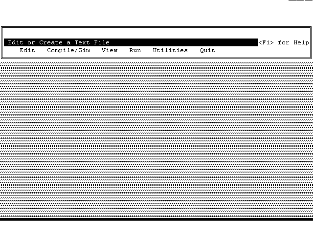
Figure 3: PLDshell Main Menu
II. Creating a Design File
This section illustrates a step-by-step tutorial on creating a digital design using PLDshell. The example design is a simple full adder targeted for an iPLD610. The process begins with a source file that must have a .PDS extension. After compilation, a JEDEC file, which is a fuse link file, is produced. Note that the complete file is included in appendix A.
Step 1: Header and Declarations
Open a source file using the Edit option. Press F6 and enter the name of the file you wish to create with the extension .PDS then press ENTER. If the file is a new one, you may use the one in Appendix A as a template. You need to modify this file to create your design file as specified below.
Create header and declarations sections that contain the following information:
TITLE Full Adder
PATTERN pds
REVISION 1.0
AUTHOR Your Name
COMPANY SUNY New Paltz
DATE Date
OPTIONS TURBO = ON ; default is on
SECURITY = OFF ; default is off
CHIP full_adder iPLD610
Step 2: Pin Names/Assignments
Modify the pin number and pin names for the design as follows (delete the unassigned pins):
;---------------------------------- PIN Declarations ---------------
; pin # label comments
;-------------------------------------------------------------------
PIN 2 cin ; carry input
PIN 3 b ; 1 bit in
PIN 4 a ; 1 bit in
PIN 5 cout ; carry out
PIN 6 sum ; sum out
PIN 12 gnd ; ground pin
PIN 24 vcc ; +5 volts
Step 3: EQUATION Section
The two outputs of the Full Adder (Sum and Cout) are implemented using Boolean equations. These equations must follow the word "EQUATIONS". The name on the left-hand side is the output name. The name and symbols on the right-hand side are the equations that implement the circuit. The following Boolean notations are used by PLDshell.
Operator Description
/ Active-Low in pin declaration; Boolean NOT elsewhere in file
* Boolean AND
+ Boolean OR
:+: Boolean XOR
= Combinational Output
*= Latched Output
:= Registered Output
![]()
![]()
![]()
![]()
![]()
The following equations need to be typed in for a Full Adder. Note that sum and carry out can be represented by ABCin + ABCin + ABCin + ABCin and AB + BCin + ACin respectively.
;----------------------------------- Equation Segment --------------
EQUATIONS
sum = a*/b*/cin + /a*b*/cin + /a*/b*cin + a*b*cin
cout = a*b + b*cin + a*cin
Step 4: Starting the SIMULATION Section
The simulation section allows you to specify a functional simulation sequence for your design. The segment follows the keyword "SIMULATION".
;----------------------------------- Simulation Segment ------------
SIMULATION
VECTOR ADD := [cin b a] ; VECTOR <name> allows you to define
; counters with bits [...] to help you
; trace program flow.
TRACE_ON cin b a cout sum ; TRACE_ON is required at the
; beginning of the simulation segment.
; It tells the simulator what pins you
; want to look at and in that order!
setf /cin /b /a ; 0+0+0 -> 00 SETF sets the inputs to 1's or 0's.
check /cout /sum ; ie. cin, b ,a
setf /cin /b a ; 0+0+1 -> 01 However, you CANNOT set the outputs.
check /cout sum ; ie. cout, sum
setf /cin b /a ; 0+1+0 -> 01
check /cout sum ; CHECK compares what the simulator
setf /cin b a ; 0+1+1 -> 10 output to what you want the output
check cout /sum ; to be. If the output isn’t the same,
setf cin /b /a ; 1+0+0 -> 01 the compiler will issue a WARNING and
check /cout sum ; the line number in which it occurred.
setf cin /b a ; 1+0+1 -> 10
check cout /sum ; The two usual causes of a WARNING
setf cin b /a ; 1+1+0 -> 10 1) a mistype in the CHECK statement.
check cout /sum ; 2) error in Boolean equation.
setf cin b a ; 1+1+1 -> 11
check cout sum ; It is confusing, looking at all the
; SETF and CHECKs. By placing a ";" at
; the end of any statement you can add
; a comment!
;
;
; comment!
TRACE_OFF ; TRACE_OFF is required at the end of
; a simulation to signal the simulator
; you're finished.
Step 5: Compiling the Design File
Save the design file and press ENTER when prompted to return to PLDshell. Press ESC key to move back to the main men.
Select the Compile/Sim option from the PLDshell main menu. Move to Accept and press ENTER or enter F10 to accept the default compile and simulation conditions. The compiler runs. The design process is finished if no error is generated and a JEDEC file must be produced. Then, skip to section IV. If there is any error, continue on to step 6.
Step 6: Viewing the Error File
Press ESC key to move back to the main men. Select the View option from the PLDshell menu, then select Error/Log Files.
Choose the error file that has the same base name as your source file with the .ERR extension and press ENTER. All error messages are displayed.
Move to the first error message and press F10. The help message for this error is displayed. The help message also recommends a course of action to correct the error.
Step 7: Revising the Source File
Press ESC three times to move back to the main menu. Use the Edit option to open the source file. Make the appropriate corrections. Save the design and exit the text editor.
Step 8: Recompiling the Design
Press ESC to move back to the main menu. Select the Compile/Sim option and recompile the design to produce a JEDEC file. Press ENTER when done to move to the main menu.
Step 9: Viewing the Simulation History File
You may view output signals generated by the simulation segment of your design file.
Select the View option from the main menu, then select Vector/Waveform Files. Choose the simulation history file for the design; this file has the same base name as your design file with .HST extension. Move to Accept and press ENTER or press F10.
View the simulation results. You can move about in the waveform by using the cursor keys. The plus "+" and minus "-" keys allow you to zoom in and out.
IV. Downloading the JEDEC File to a PLD chip
Follow the procedure specified below to download your JEDEC file to iPLD610 chip. The programmer is located in the back of WSB 105.
Step 1: Executing WACCESS program
Double click on WACCESS icon from the programmer's window. ALL-11 Universal Programmer window will open up.
Step 2: Choose PLD
Click on the DEVICE heading and choose item 6 which is PLD.
Step 3: Mfr and Type numbers
Select the desire manufacturer, in this case ALTERA, by clicking on ALTERA. Alternatively, you can key in the desired manufacturer name and press the <TAB> key. Then the type menu screen will appear.
The device type is selected in the same way as the manufacturer. You can use the mouse to click on a particular device or you can type in the device name followed by pressing the <ENTER> key. In this case you can type "EP610" followed by <ENTER> key. After selecting the correct type, click on the RUN button .
Step 4: Load JEDEC file
To load the JEDEC file from disk select "Load JEDEC File" from the "File" menu and the Load File window will open. Select your JEDEC file from you A drive and click on OK. The indicated file will be transferred to the programmer's working buffer.
Step 5: Place the chip in the socket
Simply flip the lever into the upright position, insert the chip, and flip the lever down; make sure the bottom of the chip is in the bottom of the socket. Note the notch on the drawing next to the socket. This corresponds to the notch on the chip; Pin 1 should be located on the lever side of the DIP socket. Make sure they are aligned properly.
Step 6: Blank Check
Choose this option to make sure there is no data on the chip. If it is not bank, use the Erase option to erase the data.
Step 7: Program
The program function is used to copy the contents of the working buffer to a device. Invoke the programming function by clicking the "Program" icon, or by typing P. A Programming Device window will open. Click on "OK" or press "Y" on the PC keyboard or the "YES" button on the Universal Programmer to start programming the buffer contents into the blank PLD.
Step 8: Verify
After programming the device new contents will be compared against the contents stored in the programmer's working buffer. This is called a VERIFY operation. If the contents match then the GOOD LED will light. Make sure to wait for the BUSY LED to turn off before removing the chip.
Step 9: Quit
To exit the programming process, click "Cancel" or press <ESC> to return to the main menu.
You are done!
Appendix A
A Blank Template
;PLDshell Plus/PLDasm Design Description
;---------------------------------- Declaration Segment ------------
TITLE <title>
PATTERN <pattern label>
REVISION <revision number>
AUTHOR <your name>
COMPANY SUNY New Paltz
DATE <current date>
OPTIONS TURBO = ON ; default is on
SECURITY = OFF ; default is off
CHIP <chip name> iPLD610
;---------------------------------- PIN Declarations ---------------
; pin # label comments
;-------------------------------------------------------------------
PIN 1 clk0 ; clock pin
PIN 2 in0 ; dedicated input
PIN 3 io0 ; \
PIN 4 io1 ; |
PIN 5 io2 ; |
PIN 6 io3 ; | input/output
PIN 7 io4 ; |
PIN 8 io5 ; |
PIN 9 io6 ; |
PIN 10 io7 ; /
PIN 11 in1 ; dedicated input
PIN 12 gnd ; ground pin
PIN 13 clk1 ; clock pin
PIN 14 in2 ; dedicated input
PIN 15 io8 ; \
PIN 16 io9 ; |
PIN 17 io10 ; |
PIN 18 io11 ; | input/output
PIN 19 io12 ; |
PIN 20 io13 ; |
PIN 21 io14 ; |
PIN 22 io15 ; /
PIN 23 in3 ; dedicated input
PIN 24 vcc ; +5 volts
;----------------------------------- Equation Segment --------------
EQUATIONS
;----------------------------------- Simulation Segment ------------
SIMULATION
VECTOR <name> := [ ]
TRACE_ON
TRACE_OFF
;-------------------------------------------------------------------
Appendix B
Full Adder
;PLDshell Plus/PLDasm Design Description
;---------------------------------- Declaration Segment ------------
TITLE Full Adder
PATTERN pds
REVISION 1.0
AUTHOR Baback Izadi
COMPANY SUNY New Paltz
DATE March 1999
OPTIONS TURBO = ON ; default is on
SECURITY = OFF ; default is off
CHIP full_adder iPLD610
;---------------------------------- PIN Declarations ---------------
; pin # label comments
;-------------------------------------------------------------------
PIN 2 cin ; carry input
PIN 3 b ; 1 bit in
PIN 4 a ; 1 bit in
PIN 5 cout ; carry out
PIN 6 sum ; sum out
PIN 12 gnd ; ground pin
PIN 24 vcc ; +5 volts
;----------------------------------- Equation Segment --------------
EQUATIONS
sum = /cin*/b*a + /cin*b*/a + cin*/b*/a + cin*b*a
cout = cin*b + cin*a + b*a
;----------------------------------- Simulation Segment ------------
SIMULATION
VECTOR ADD := [cin b a] ; VECTOR <name> allows you to define
; counters with bits [...] to help you
; trace program flow.
TRACE_ON cin b a cout sum ; TRACE_ON is required at the
; beginning of the simulation segment.
; It tells the simulator what pins you
; want to look at and in that order!
setf /cin /b /a ; 0+0+0 -> 00 SETF sets the inputs to 1's or 0's.
check /cout /sum ; ie. cin, b ,a
setf /cin /b a ; 0+0+1 -> 01 However, you CANNOT set the outputs.
check /cout sum ; ie. cout, sum
setf /cin b /a ; 0+1+0 -> 01
check /cout sum ; CHECK compares what the simulator
setf /cin b a ; 0+1+1 -> 10 output to what you want the output
check cout /sum ; to be. If the output isn’t the same,
setf cin /b /a ; 1+0+0 -> 01 the compiler will issue a WARNING and
check /cout sum ; the line number in which it occurred.
setf cin /b a ; 1+0+1 -> 10
check cout /sum ; The two usual causes of a WARNING
setf cin b /a ; 1+1+0 -> 10 1) a mistype in the CHECK statement.
check cout /sum ; 2) error in Boolean equation.
setf cin b a ; 1+1+1 -> 11
check cout sum ; It is confusing, looking at all the
; SETF and CHECKs. By placing a ";" at
; the end of any statement you can add
; a comment!
;
; comment!
TRACE_OFF ; TRACE_OFF is required at the end of
; a simulation to signal the simulator
; you're finished.
Appendix C
0 to 9 Synchronous Counter
;-------------------------------------------------------------------
;PLDshell Plus/PLDasm Design Description
;---------------------------------- Declaration Segment ------------
TITLE Sample MOD-10 Counter (0-9)
PATTERN pds
REVISION 1.0
AUTHOR Baback Izadi
COMPANY SUNY New Paltz
DATE March 1999
OPTIONS TURBO = ON ; default is on
SECURITY = OFF ; default is off
CHIP counter iPLD610
;---------------------------------- PIN Declarations ---------------
; pin # label comments
;-------------------------------------------------------------------
PIN 1 clk0 ; clock pin
PIN 2 reset ; Asynchronous reset pin
PIN 3 clkout ; to clock another
PIN 4 d ; Most significant bit of the counter
PIN 5 c
PIN 6 b
PIN 7 a ; Least significant bit of the counter
PIN 12 gnd ; ground pin
PIN 24 vcc ; +5 volts
;----------------------------------- Equation Segment --------------
EQUATIONS
; IMPORTANT: combinational equations use "=" and sequential equations use":=".
d.d := d*/a+c*b*a ; All registered output pins have extensions
d.rstf = /reset ; to define special functions of the output
c.d := /c*b*a+c*/b+c*/a ; .aclk = asynchronous clock
c.rstf = /reset ; .clkf = synchronous clock
; .trst = output enable equation
b.d := /d*/b*a+/d*b*/a ; .rstf = clear equation
b.rstf = /reset ; .setf = preset equation
; .d = data input to D-type register
a.d := /a ; .t = data input to T-type register
a.rstf = /reset ; .j = J data input to JK register
; .k = K data input to KJ register
clkout.d := d*a ; .r = R data input to SR register
clkout.rstf = /reset ; .s = S data input to SR register
;----------------------------------- Simulation Segment ------------
SIMULATION
VECTOR count := [d c b a] ; VECTOR <name> allows you to define
TRACE_ON reset clkout d c b a ; counters with bits [...] to help you
; trace program flow.
; TRACE_ON is required at the
; beginning of the simulation segment.
; It tells the simulator what pins to
; look at and in that order!
setf /reset /clk0
check /clkout /d /c /b /a ; 0 SETF sets the inputs to 1's or 0's.
setf reset ; i.e. reset.
clockf clk0 ; However you CANNOT set the outputs.
check /d /c /b a /clkout ; 1 ie. d, c, b, a, clkout.
clockf clk0
check /d /c b /a /clkout ; 2 CLOCKF tells the simulator to toggle
clockf clk0 ; or pulse the input.
check /d /c b a /clkout ; 3 ie. +5V
clockf clk0 ; 0V OR
check /d c /b /a /clkout ; 4
clockf clk0 ; PRLDF sets the registers inside the
check /d c /b a /clkout ; 5 EPLD610.
clockf clk0
check /d c b /a /clkout ; 6 CHECK compares what the simulator
clockf clk0 ; output to what you want the output
check /d c b a /clkout ; 7 to be. If the output isn't the same
clockf clk0 ; the compiler will issue a WARNING
check d /c /b /a /clkout ; 8 and the line number at which it
clockf clk0 ; occurred.
check d /c /b a /clkout ; 9
clockf clk0 ; The two usual causes of a WARNING.
check /d /c /b /a clkout ; 0 1) a mistype in the check statement.
; 2) error in Boolean equation.
; It is confusing looking at all the
; SETF and CHECKs. By placing a ";" at
; the end of any statement you can add a comment!
![]()
; comments!
TRACE_OFF ; TRACE_OFF is required at the end of
; a simulation to signal the simulator
; you're finished.
;-------------------------------------------------------------------